A high dynamic range of this click allows it to be used for very precise sampling of the input voltage between A+ and A-, as it allows detection of changes down to a magnitude of few nanovolts. ADC 7 click accepts a differential voltage on the input terminal, which results in a robust and clean signal path. All these features allow this device to be used for developing various applications, including seismology applications, high precision instrumentation applications, energy exploration applications, and similar sensitive applications that require very high sampling accuracy.
How does it work?
ADC 7 click uses the advanced ADC IC, labeled as LTC2500-32. It is a 32-bit oversampling ADC with a configurable digital filter, from Analog Devices. The integrated configurable filter is used to process the data from the 32bit successive approximation register (SAR) core, providing a very low noise on the output, with the high dynamic range up to 148dB. It also simplifies the design, as it relaxes anti-aliasing filter requirements for the input signal. The LTC2500-32 ADC also allows external reference voltage to be used, therefore the Click board™ provides it with 4.096 V from a tiny fixed reference voltage IC from Microchip, labeled as MCP1541.
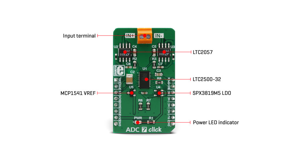
There is a two-pole screw terminal on the Click board™, with its inputs routed to +IN and -IN pins of the ADC IC. The input signal can be bipolar, unipolar, and differential, swinging from 0 to VREF. Inputs are buffered with two LTC2057 operational amplifiers. These low-noise op-amps are used to adjust the impedance of the input, as the LTC2500-32 ADC performs optimally when driven with low impedance sources. The inputs are DC coupled - no decoupling capacitors are used on the input signal path.
The LTC2500-32 has two SDO pins available (dual SPI interface), yet only SDOA pin is used on this Click board™, offering conversion data from the programmable digital filter. To initiate the SPI communication, RDLA pin should be set to a LOW logic level. It is routed to the CS pin of the mikroBUS™, while the SDOA pin is routed to the MISO pin of the mikroBUS™, labeled as SDO. Configured like this, it is possible to use the standard four-pin SPI interface of the mikroBUS™ to communicate with the Click board™.
The digital filter can be either programmed via the SPI interface (SDI pin of the mikroBUS™), or it can use the PRE pin of the ADC IC. When the PRE pin is set to a HIGH logic level, a logic state on the SDI pin will be used to select one of two filter presets. Otherwise, when the PRE pin is set to a LOW logic level, the filter can be configured via the SPI interface. PRE pin is routed to the RST pin of the mikroBUS™ and labeled as PRE.
This IC uses an external signal to initiate the conversion process. When a rising edge appears on the MCLK pin, the internal conversion process is started. For the optimal performance, the manufacturer recommends that the external signal pulse duration should be 40nS. The MCLK pin is routed to the PWM pin of the mikroBUS™ and is labeled as MCK.
After a rising edge on the MCLK pin, the ADC starts sampling phase by comparing the input voltage with the binary-weighted fractions of the reference voltage. The sampled input is then passed through the successive approximation algorithm (SAR ADC type). The conversion data is composed of 24 bits for the differential voltage, 7 bits for the common mode voltage, and one flag bit used as a signal overflow indicator (VIN > VREF). This data is then passed to the filter section, which stores a 32-bit processed value on the output register. The ADC IC compares the differential input voltage with the 2 × VREF, divided into 232 levels, resulting in a 1.9mV resolution (using 4.096V as a reference). The wide common-mode input range (from 0V, up to VREF), coupled with the high common mode rejection rate, allows all types of signals to be sampled by the device: pseudo-differential unipolar, pseudo-differential bipolar, and fully differential. It is a unique feature of the LTC2500-32 ADC device.
During the conversion phase, the BUSY pin is kept at HIGH logic level (Hi-Z). When the conversion ends, this pin is driven to a LOW logic level. The BUSY pin indicates the conversion-in-progress state and it is routed to the mikroBUS™ INT pin, labeled as BSY. Another pin of the LTC2500-32 ADC with similar function indicates that there is a data ready to be read at the output register. This pin is labeled as DRL and it is routed to the mikroBUS™ AN pin. By using these pins as the interrupt sources, the host MCU is allowed to achieve optimized data acquisition timing, not having to poll the ADC until it gets ready.
The Click board™ uses both 3.3V and 5V rails of the mikroBUS™.The 3.3V rail is used to provide the operating voltage for the ADC IC, which is 2.5V. Therefore, a small LDO is used to obtain this voltage. The 5V rail of the mikroBUS™ is used as the input voltage for the MCP1541 reference voltage source. Since the logic section of the LTC2500-32 ADC can operate with voltages from 1.8V up to 5V, no additional communication level shifting ICs are required, and the Click board™ can operate with both 3.3V and 5V MCUs.
About filters and aliasing
When sampling high-frequency signals, a phenomenon called aliasing occurs. This is a phenomenon in which a new waveform with lower frequency, not present in the input signal, is generated at the ADC output because as the input signal frequency gets closer to a sampling frequency, fewer samples can be taken to faithfully represent the input signal. At frequency equal to half of the sampling frequency, there is only one sample that can be made for each half-cycle of the input signal. This frequency is called a Nyquist frequency.
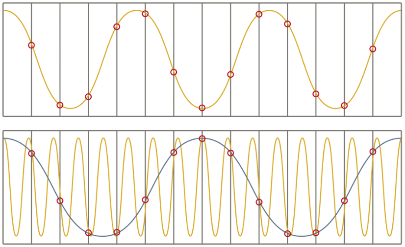
Aliasing occurs as the result of a much lower sampling frequency
To cope with this problem, the input signal needs to be limited to a region under this frequency, yet it must not attenuate the useful signal. To achieve such a task, an input filter with the high Q factor - a steep slope of its characteristic, is required. This implies using higher order filters, which additionally complicate the design, since building analog filters of higher order is not a simple task.
Some advanced solutions come in a form of DSPs and FPGAs, offering digital filters, that can achieve very steep slopes of their filter characteristics. The LM2500-32 ADC offers an integrated filtering section with seven different filter types, optimized for anti-aliasing purposes. This simplifies the circuit design, requiring only a simple first or second order filter at the input, yet offering great antialiasing results. More in-depth information about filters can be found in the LM2500-32 datasheet.
Specifications
| Type |
ADC |
| Applications |
It can be used for developing various applications, including seismology applications, high precision instrumentation applications, energy exploration applications, and similar sensitive applications that require very high sampling accuracy |
| On-board modules |
LTC2500-32, a 32-bit oversampling ADC with a configurable digital filter, from Analog Devices; LTC2057, a high voltage, low noise, zero-drift operational amplifier, from Analog Devices |
| Key Features |
Seven types of integrated digital filters with programmable options, 32-bit data output with high dynamic range, wide range of common mode voltage allows different kinds of bipolar and unipolar input signals to be sampled, and more |
| Interface |
SPI |
| Click board size |
M (42.9 x 25.4 mm) |
Pinout diagram
This table shows how the pinout on ADC 7 click corresponds to the pinout on the mikroBUS™ socket (the latter shown in the two middle columns).
| Notes | Pin |  | Pin | Notes |
|---|
| Data Ready Indicator |
DRL |
1 |
AN |
PWM |
16 |
MCK |
Sampling Trigger |
| Filter Preset Enable |
PRE |
2 |
RST |
INT |
15 |
BSY |
Busy Indicator |
| Chip Select |
CS |
3 |
CS |
RX |
14 |
NC |
|
| SPI Clock |
SCK |
4 |
SCK |
TX |
13 |
NC |
|
| SPI Data-Out |
SDO |
5 |
MISO |
SCL |
12 |
NC |
|
| SPI Data In/Preset Sel |
SDI |
6 |
MOSI |
SDA |
11 |
NC |
|
| Power supply |
3.3V |
7 |
3.3V |
5V |
10 |
5V |
Power supply |
| Ground |
GND |
8 |
GND |
GND |
9 |
GND |
Ground |
Onboard settings and indicators
| Label | Name | Default | Description |
|---|
| PWR |
PWR |
- |
Power LED indicator |
| TB1 |
IN+, IN- |
- |
Input signal connection terminal |
Software support
We provide a library for the ADC 7 Click on our LibStock page, as well as a demo application (example), developed using MikroElektronika compilers. The demo can run on all the main MikroElektronika development boards.
Library Description
The library can perform 32bit AD conversion and can read this 32bit converted voltage value with or without configuration byte/bytes. Library also offers a choice to set configuration for the next conversion cycles. It is not necessary to set configuration for each conversion. A user always can perform conversion cycle/cycles with the last entered configurations. The user can read the converted voltage value as 32bit digital value or as a value calculated in the mV unit. For more details check the documentation.
Key functions:
uint8_t adc7_setConfig( uint8_t gainConfig, uint8_t downSampFactor, uint8_t filterType ) - The function performs the device configuration by sending configuration data to configure the next conversion cycle.
void adc7_startConvCycle( void ) - The function generates the clock signal on MCK pin and on that way starts and performs the desired number of conversion cycles, determined by Down Sampling Factor number.
uint8_t adc7_readResults( int16_t *voltage ) - The function reads 32bit converted voltage value from A/D converter and calculates this value to mV.
Example description
The application is composed of three sections :
- System Initialization - Initializes peripherals and pins.
- Application Initialization - Initializes SPI interface and performs configuration for conversion cycles.
- Application Task - (code snippet) - Performs the determined number of conversion cycles which are necessary for averaging.
void applicationTask()
{
 adc7_startConvCycle();

 while (adc7_checkDataReady() == _ADC7_DATA_NOT_READY);

 adc7_readResults( &voltageData );

 LongToStr( voltageData, text );
 mikrobus_logWrite( "Voltage: ", _LOG_TEXT );
 mikrobus_logWrite( text, _LOG_TEXT );
 mikrobus_logWrite( "mV", _LOG_LINE );

 Delay_ms( 200 );
}
The full application code, and ready to use projects can be found on our LibStock page.
Other mikroE Libraries used in the example:
Additional notes and information
Depending on the development board you are using, you may need USB UART click, USB UART 2 click or RS232 click to connect to your PC, for development systems with no UART to USB interface available on the board. The terminal available in all MikroElektronika compilers, or any other terminal application of your choice, can be used to read the message.
mikroSDK
This click board is supported with mikroSDK - MikroElektronika Software Development Kit. To ensure proper operation of mikroSDK compliant click board demo applications, mikroSDK should be downloaded from the LibStock and installed for the compiler you are using.
For more information about mikroSDK, visit the official page.